I still remember my third year of undergrad as an electrical engineering major — the time we first dipped our toes into digital circuit design using hardware description languages. The HDLs themselves weren’t too bad once you got the hang of them, but getting those circuits to actually run on an FPGA? That was straight-up chaos. We were using Altera FPGAs with the Quartus IDE on Linux machines, and just getting the software and drivers to play nice felt like solving a puzzle designed by someone who hates you. Somehow, we stumbled our way through that course, and I was more than happy to leave FPGAs behind as I dove into semiconductor device research for my PhD at MIT. But as fate would have it (plot twist!), I recently found myself circling back into the FPGA vortex for a new project. All I had were distant, mildly traumatic memories of the ordeal — no actual memory of how to make anything work.
So here we are again. I had to relearn everything from scratch, piecing it together step by step and hoping I’m not just reinventing a more chaotic wheel. This blog is my way of documenting those steps — implementing a fairly simple digital design on an FPGA — so Future Me (and maybe Present You, curious reader) can skip the unnecessary suffering next time around. Oh, and by the way: the Mersenne Twister (MT) pseudo-random number generator is just the guinea pig for this project. If you're here for a deep dive into PRNG metrics, this probably isn’t your ride. But if you're looking to get a basic design up and running on an FPGA without losing your mind — welcome aboard.
I’ll start with a quick primer on the Mersenne Twister — just enough to give you a feel for how the FSM ticks, so the Verilog code that follows actually makes some sense. Once that’s out of the way, we’ll dive into the simulation workflow: from basic behavioral simulation to the post-implementation stage. After that, I’ll walk through how to get solid, high-confidence energy estimates using Vivado’s Power Report tool, with the help of a SAIF (Switching Activity Interchange Format) file. At this point, the FPGA will be happily generating MT19937 pseudo-random numbers internally. But unless you’re planning to sit and stare at LED blinks for entropy, we’ll need to slap on a UART transmitter to stream the numbers to a PC for verification. With that UART wrapper in place, we’ll be all set to flash the code and watch a stream of Mersenne magic roll out of the FPGA.
A Quick Tour of the MT19937
The Mersenne Twister is a widely-used pseudo-random number generator (PRNG) known for its long period and high-quality randomness. The "19937" part in MT19937 refers to the fact that its period is \( 2^{19937}−1 \), which is a very large prime number — specifically, a Mersenne prime. This extremely long period ensures that the generator produces a sequence of numbers with minimal repetition, making it well-suited for applications requiring high-quality randomness. The original publication detailing the method can be found here.
Here’s the high-level breakdown of how MT19937 works:
- Seeding: A 624-word internal state is initialized using a recurrence formula, starting from a single external seed.
- Twisting: New state values are generated in chunks using XORs, shifts, and a conditional matrix multiply with a constant matrix_a.
- Tempering: The raw output from the twist is passed through a series of XOR-and-shift operations to improve statistical quality.
The FSM

To coordinate all this logic, I designed a finite state machine (FSM) that cycles through four states:
- S0 – IDLE: Waiting for the ext_seed_enable signal. This is the FPGA equivalent of twiddling thumbs.
- S1 – SEED: Seeds the internal 624-entry state array using a recurrence. Outputs done_seed = 1 when finished.
- S2 – TWIST: Executes the twisting transformation. At each cycle, it:
- Grabs three words from the state array,
- Computes a twisted value via masked bit operations and XORs,
- Applies tempering to the result,
- Produces a final random_number and raises the valid_rn flag.
- S3 – TRANSIT: A guard band between SEED and TWIST to ensure memory operations complete cleanly.
The transitions between states are driven by the done_seed and done_twist flags. Once initialized, the FSM loops between twisting and reseeding, generating new outputs on every cycle of the twisting phase.
Module Breakdown: Who Does What
Here’s how the Verilog modules are sliced up:
mt_fsm.v: The central controller. It handles all state transitions and control signals for the rest of the design, in accordance with the FSM described above.
mt_seed.v: Responsible for seeding the MT state array. It iterates through all 624 indices, calculating and writing new values using the initialization recurrence. When done, it asserts done_seed.
mt_twist.v: This one handles the core of the algorithm. For each cycle:
- It calculates the new twisted value using neighboring entries of the state array.
- Performs the tempering step using constants from the MT19937 specs.
- Outputs a valid 32-bit pseudo-random number and writes the updated state back.
mt_state_mem.v: A dual-ported memory array with 624 words of 32-bit state. Both the seed and twist modules read/write to it based on the FSM’s control.
Together, these modules recreate the MT19937 algorithm step by step, entirely in hardware. It’s overkill if you just want to generate random numbers — but gold if you care about deterministic, cycle-accurate, energy-measurable randomness for hardware benchmarking (which I do).
Running the Behavioral simulation
As the name suggests, behavioral simulation is about verifying whether your digital design "behaves" as intended — before you go anywhere near actual hardware. For the Mersenne Twister implemented here, the goal of simulation is to check whether the FSM cycles correctly between seeding the state memory and performing the twist/temper operation, and whether the output random_number stream looks valid — ideally, uniform over the 32-bit range. What makes this process powerful is the waveform database: it logs how every signal in your design changes over time. This becomes an essential tool for debugging, letting you visually trace issues like stuck states, incorrect transitions, or invalid outputs — long before you flash anything onto an FPGA.
To run a behavioral simulation, you need to write a "testbench" — a kind of wrapper module that mimics the real-world environment your design would operate in. The testbench doesn’t get synthesized or loaded onto the FPGA. Its only job is to stimulate your design with clock signals, resets, and inputs, and to observe outputs, just like a virtual lab setup.
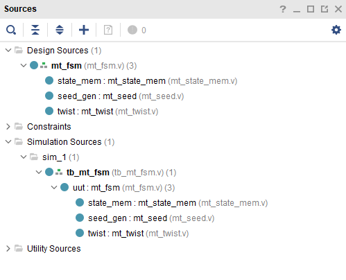
In this project, the testbench file tb_mt_fsm.v instantiates the top-level module mt_fsm. It drives the clk and rst lines, provides an external_seed value, and toggles the external_seed_enable flag to kick off the FSM. It also captures the output signals random_number and valid_rn, and writes the random numbers to a text file so we can inspect them offline.
At this stage, the project files hierarchy in Vivado should look something like the screenshot below - mt_fsm.v is the top-level Design Source and tb_mt_fsm.v is the top-level Simulation Source. With that verified, we can simply go to Simulation >> Run Simulation in the Project Manager on Vivado and click Run Behavioral Simulation to trigger the simulation.
Post-implementation simulation and Power Report generation
By this point, the behavioral simulation has verified that the design works as expected. But before flashing it onto the FPGA, it’s wise to run a few more checks. We want to know whether the design will operate reliably at the target clock frequency, how much power it might consume, and whether it risks heating up during sustained operation. These questions are addressed through Vivado’s Synthesis and Implementation stages. Once Implementation completes, Vivado provides a Utilization Report that tells us how many FPGA resources — like LUTs, flip-flops, and DSPs — the design consumes. It also generates a Timing Report, where metrics like the Worst Negative Slack and Worst Hold Slack let us assess whether the design meets timing requirements.
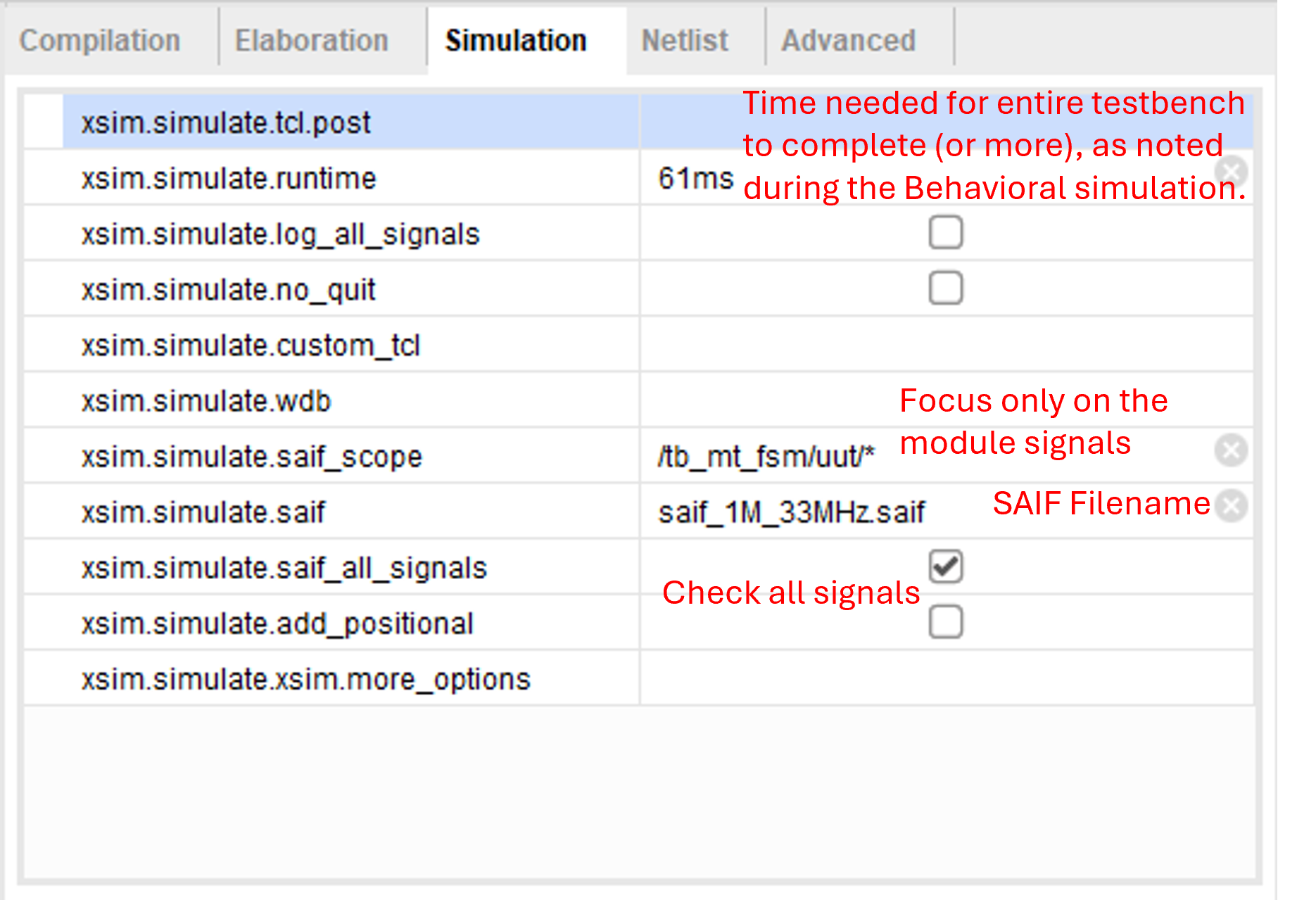
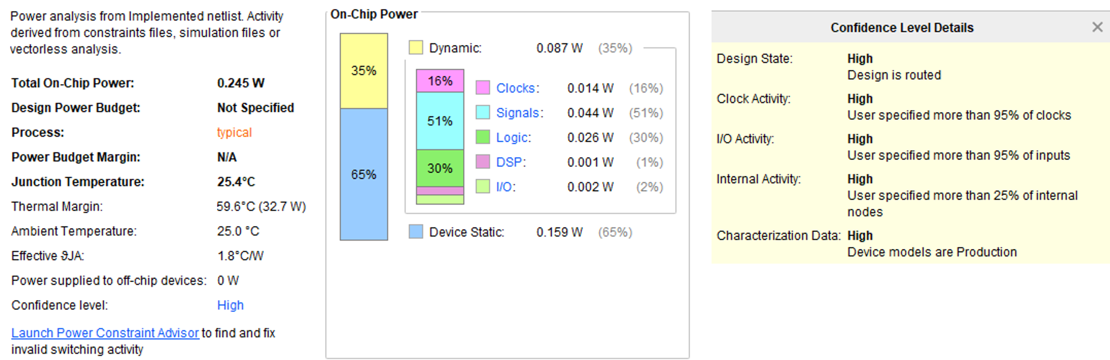
Vivado also provides a Power Report at this stage, but the numbers in that report are based on internal heuristics about signal switching activity. In other words, it makes educated guesses about how often each signal toggles per second. This can be misleading, especially for designs like a pseudo-random number generator, where some signals might switch very frequently while others rarely do. To improve accuracy, we can generate a SAIF file — a Switching Activity Interchange Format file — that records actual signal transitions during a Post-Implementation Functional Simulation. This simulation uses the same design and testbench as before, but with the added instructions for Vivado to track how many times each signal flips. Once the simulation runs long enough — say, until one million random numbers have been generated — we end up with a detailed and realistic estimate of each signal’s activity. Feeding this SAIF file back into Vivado lets the tool refine its Power Report, giving you a much more trustworthy estimate of your design’s real-world power consumption. To enable logging a SAIF file, we can use the Simulation Settings, and populate the required details as shown below.
Additionally, we must specify a clock constraint to allow timing analysis during Implementation. This can be done by simply adding a constraints.xdc file to the project as a Constraints source, and the file just needs one line of code
create_clock -name clk -period 30.000 [get_ports {clk}];Here, the period is specified in nanoseconds. With the SAIF related settings done and the clk constraint defined, we can now proceed to run the Post-Implementation Functional Simulation. Once the simulation is complete, the SAIF file can be fed to Vivado's Power Report dialog box which then generates a detailed, high-confidence estimate of our design's power consumption at the specified clock frequency.
Preparing for FPGA deployment - Clocks, Comms and Constraints
Having verified that the design behaves as expected and gathered useful reports on timing, resource utilization, and power consumption, the next step is to prepare the design for deployment onto the FPGA. At a basic level, this involves updating the constraints file to map the ports of the top-level Verilog module to the actual I/O pins of the FPGA — and by extension, to the development board’s peripherals like LEDs, switches, buttons, or UART interfaces. However, for this project, I made a few additional changes specific to the Genesys2 board to properly handle its differential clock input and ensure UART-based streaming of the random number output to a PC.
The Genesys2 board provides a differential clock source running at 200 MHz, whereas my Mersenne Twister design expects a single-ended clock input. To bridge this, I created a new top-level module, mt_uart.v, which first takes in the differential clock pair, comprising sysclk_p and sysclk_n, and converts it to a single-ended clock, clk, using an input buffer. This resulting clock signal, still at 200 MHz, is then downsampled to a lower frequency (seq_clk) suitable for driving the FSM. The downsampling is done using a simple counter-based divider, while the conversion from differential to single-ended clock uses the following Verilog snippet, which is standard for Xilinx-based boards:
    // === Differential Clock Buffer ===
    wire clk;
    IBUFDS #(
        .DIFF_TERM("TRUE"),
        .IBUF_LOW_PWR("FALSE")
    ) clk_ibuf (
        .O(clk),
        .I(sysclk_p),
        .IB(sysclk_n)
    );
With the clocks configured, the digital design is in principle ready to happily generate 32-bit random numbers inside the FPGA — but we need a way to actually see those numbers on a computer. That’s where UART (Universal Asynchronous Receiver/Transmitter) comes in. UART is one of the simplest and most widely used serial communication protocols for talking to microcontrollers, FPGAs, or pretty much any embedded device. Physically, it uses just two wires - Rx and Tx. It's asynchronous, meaning there’s no clock line shared between sender and receiver — both ends just agree on a baud rate (bits per second) and stick to it. Each byte is sent as a packet that includes:
That makes each byte a 10-bit packet on the wire.
To send the MT19937-generated numbers to the PC, I wrote a uart_tx.v module. It takes in 1 byte from a register and handles all the UART-level packing: adding the start and stop bits, and shifting the bits out serially on a tx line. It also has a busy flag so the controller knows when to wait before sending the next byte.
Then comes the new top-level module, mt_uart.v. This one connects the dots:
So for every new random number generated, four UART packets are streamed out to the PC.
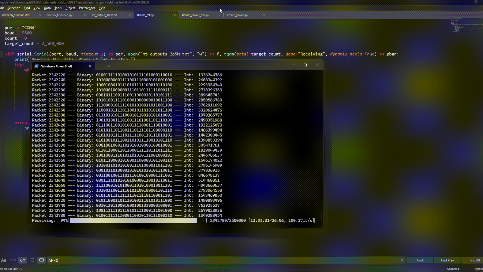
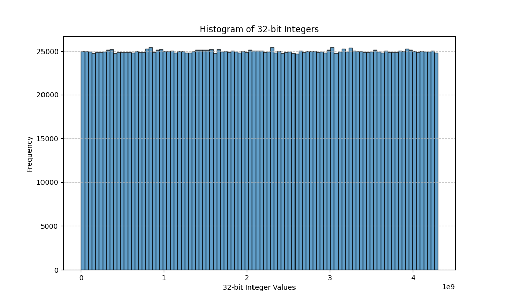
On the PC side, I wrote a short Python script (stream_mt.py) using the pyserial library. It listens to the serial port, grabs the incoming bytes, assembles them back into 32-bit words, and writes them into a text file — one number per line. This gives me a quick and easy way to verify that the MT output looks reasonable (or at least non-repeating!) and also lets me analyze the distribution offline.
Finally, to make the design physically compatible with the Genesys2 board, we need to define how the logical ports in our Verilog code map to the actual FPGA pins. This is done in the constraints file (.xdc), where we also specify the electrical standards for each I/O and create a named clock. Below is the constraints snippet used in this project — it assigns the differential system clock, a reset button, LEDs for displaying the FSM state, and the UART transmit pin for streaming random numbers to the PC.
## Clock Signal
set_property -dict { PACKAGE_PIN AD11  IOSTANDARD LVDS     } [get_ports { sysclk_n }]; #IO_L12N_T1_MRCC_33 Sch=sysclk_n
set_property -dict { PACKAGE_PIN AD12  IOSTANDARD LVDS     } [get_ports { sysclk_p }]; #IO_L12P_T1_MRCC_33 Sch=sysclk_p
create_clock -name sysclk -period 5.000 [get_ports {sysclk_p}]

## Buttons
set_property -dict { PACKAGE_PIN R19   IOSTANDARD LVCMOS33 } [get_ports { reset }]; #IO_0_14 Sch=cpu_resetn

## LEDs
set_property -dict { PACKAGE_PIN T28   IOSTANDARD LVCMOS33 } [get_ports { disp_state[0] }]; #IO_L11N_T1_SRCC_14 Sch=led[0]
set_property -dict { PACKAGE_PIN V19   IOSTANDARD LVCMOS33 } [get_ports { disp_state[1] }]; #IO_L19P_T3_A10_D26_14 Sch=led[1]
set_property -dict { PACKAGE_PIN U30   IOSTANDARD LVCMOS33 } [get_ports { disp_state[2] }]; #IO_L15N_T2_DQS_DOUT_CSO_B_14 Sch=led[2]
set_property -dict { PACKAGE_PIN U29   IOSTANDARD LVCMOS33 } [get_ports { disp_state[3] }]; #IO_L15P_T2_DQS_RDWR_B_14 Sch=led[3]
set_property -dict { PACKAGE_PIN V20   IOSTANDARD LVCMOS33 } [get_ports { disp_state[4] }]; #IO_L19N_T3_A09_D25_VREF_14 Sch=led[4]
set_property -dict { PACKAGE_PIN V26   IOSTANDARD LVCMOS33 } [get_ports { disp_state[5] }]; #IO_L16P_T2_CSI_B_14 Sch=led[5]
set_property -dict { PACKAGE_PIN W24   IOSTANDARD LVCMOS33 } [get_ports { disp_state[6] }]; #IO_L20N_T3_A07_D23_14 Sch=led[6]
set_property -dict { PACKAGE_PIN W23   IOSTANDARD LVCMOS33 } [get_ports { disp_state[7] }]; #IO_L20P_T3_A08_D24_14 Sch=led[7]

## UART
set_property -dict { PACKAGE_PIN Y23   IOSTANDARD LVCMOS33 } [get_ports { tx }]; #IO_L1P_T0_12 Sch=uart_rx_out
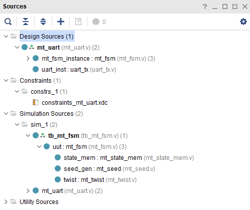
With the new design sources and the constraint file added, the project herarchy looks something like this:
Fire away!
Well, all our preparations are finally done! Just head over to Vivado's Project Manager and run Synthesis, Implementation, and Generate Bitstream in sequence. Once the bitstream is ready, flash it onto the FPGA using Vivado's Hardware Manager. You should see the LEDs spring to life — a visual confirmation that the Mersenne Twister is up and running on hardware.
Now, to start collecting those random numbers, open your terminal and run the stream_mt.py Python script. That’s it. The whole setup is live, generating and streaming high-quality pseudo-random numbers straight from your FPGA to your PC.
If you’ve read this far, thanks for following along. If you spotted anything off, have suggestions to make things better, or just want to say hi and share your own experiences, I’d be genuinely happy to hear from you. Drop a message, a comment, or even a random number — I’m listening.